As the use of various electronic components, such as sensors, displays and lights within the final projects can result in a mess of wires and cable management, it is appropriate to simplify the circuitry using a custom designed PCB. This is especially useful, as the case’s components are meant to be largely independent of the motherboard and power supply used inside of it and the reduction of cable management increases servicability and airflow.
And of course, all project files are available for download1
However, for production environments you’d usually try to get everything printed onto the same board, such that everything is simplified towards your specific design goals without unnecessary excess. Because of this I will outline a process of designing a PCB around the Atmel ATTINY44 (which is a chip commonly used in Arduino controllers) using Autodesk EAGLE.
Before we can start, we need to set up our environment. There are many PCB design tools out there both libre and commercial, but for the sake of simplicity I decided to go with Autodesk EAGLE, which unlike Fusion 360 is shipped in a feature-limited rather than time-limited trial version and also features native Linux support.
Once EAGLE is installed and we created the first project, we need to import a few parts we need to use on our PCB. For this we need to open the library manager and add the necessary files for the FAB2 and Fab_Hello3 libraries respectively.
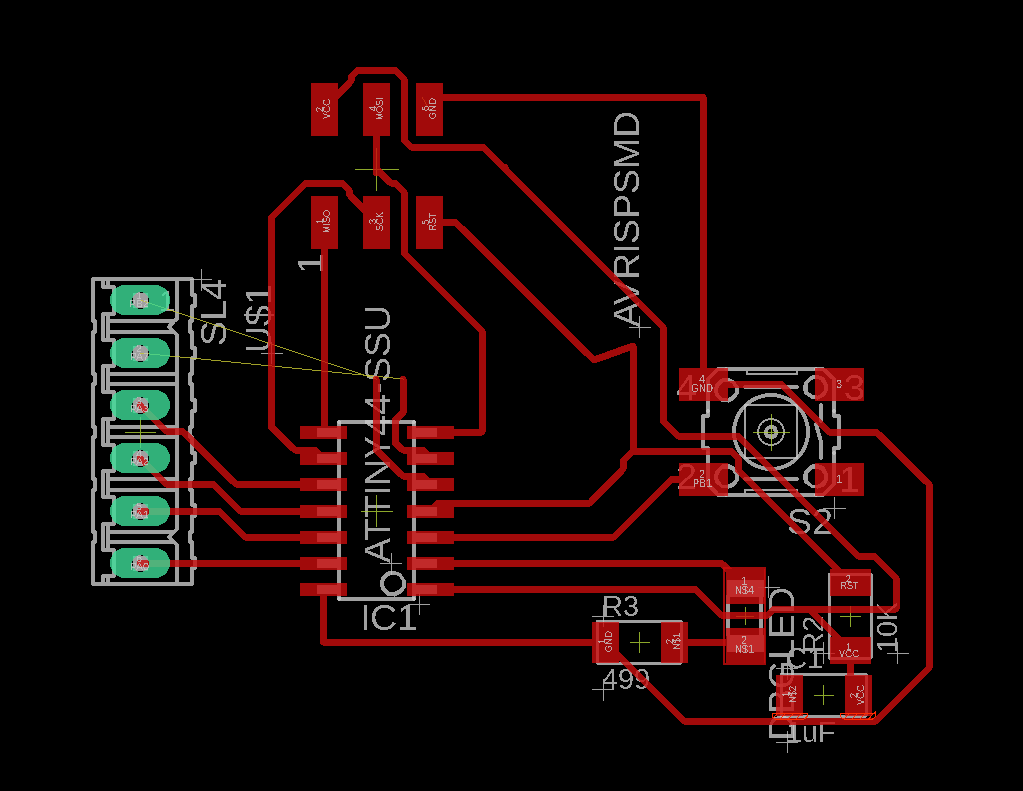
The final schematic ended up quite simple, so I think I can explain it entirely using the image below:
These labels you see are called XRefs. they are a feature of EAGLE which allows you to logically wire together multiple connections without visually representing then, reducing clutter.
Anyway, first I set the obligatory VCC and GND connections as well as wire a 1uF capacitor into it to keep. You can see those in the top left corner.
Below you can find an AVRISPSMD, which is an input plug through which the ATTINY44 can be accessed. I wired all ports according to their appropriate connections to the ATTINY44. More on that later.
As the ATTINY44-SSU’s reset is triggered on PB3 being closed LOW, I connected a pullup VCC connection as well as a reset connector, such that it only gets reset on user input.
I also wired in an LED into PB0 to serve as an Arduino pin 13-esque debug light for programmers. All other pins were either wired according to the AVRISPSMD plug or smiply wired into an output array (MO6).
For this exercise we settle on a machine that is capable of creating traces of at least 12mil thickness with an atmil of 16mil. The unit mil, contrary to common belief does not signify a measurement in milimeters here, but rather 1/100th of an inch. In the Image below you can see my solution for the traces:
Sadly as the atmil was not precise enough, I ended up not being able to connect the output pins PA7 and PB2 (loose traces in the middle), as there is logically no safe way to connect these without the use of a 2nd layer.
After a while I decided to use a Polygon to automatically fill in all necessary GND connections and split the accessible connections into PA0-3 and PA7/PB2 and following lots of trial and error, here’s the final result